はじめに
VHDLを初めて習う人のために,手元で動かせる簡単なシミュレーションについていくつか紹介してみたい.シミュレーションの準備については,
に GHDL を gtkwave の環境構築の方法を説明したので,こちらを参考にしてほしい.(vivado や modelsim などの高度なソフトウェア環境が整っている場合は,そちらでも構いませんが,ほんとに基本的なことをVHDLの文法や機能を確認したいだけにしては,起動も遅いし,高度すぎるので,自分の場合は,GHDL+gtkwave の組合せが一番フィットしました.)
参考ページとして,https://vhdlwhiz.com が物凄く丁寧に紹介しているので,一度立ち寄ってほしい.主催者は,2018年に転職した折に作り始めたページのようであるが,趣味のレベルは超えてる気がする..
基本はすでに習得済みの人で、トリガーをかけたいとか思ってる人は、
を参照ください。
最初の一歩 : clock の生成
コード
まずは,一番の基本になるクロックを生成してみよう.周波数は100MHzとしよう.
library ieee;
use ieee.std_logic_1164.all;
use ieee.numeric_std.all;

entity clock_tb is
end entity;

architecture sim of clock_tb is

    constant ClockFrequency : integer := 100e6; -- 100 MHz
    constant ClockPeriod    : time    := 1000 ms / ClockFrequency;
    signal Clk : std_logic := '1';

begin
    -- Process for generating the clock
    Clk <= not Clk after ClockPeriod / 2;

    -- Testbench sequence
    process is
    begin
    	wait for 50 ns;
        assert (false) report "Simulation End!" severity failure;
        wait;
    end process;

end architecture;
細かいことが色々あるが,クロックを生成しているのは,
Clk <= not Clk after ClockPeriod / 2;
の部分だけである.ここで,ClockPeriod は,100MHzのクロックを周期が10nsなので,5ns ごとに,クロックのビットを 1 -> 0 -> 1 -> ... と切り替えることになる.1(立ち上がり) -> 0(立ち下がり) の2つのセットを"1クロック" と考えるので,5ns ごとに切り替えることになる.
それだけ?のことあるが,クロックの立ち上がりだけで動くシステムも作れるし,立ち上がりと立ち上がりの両方で動くシステムも作ることができて,動く周波数がそれだけで2倍かわるので大きい違いではある.例えば,クロックの立ち上がりと立ち下がりの両エッジで動くDouble Data Rate (DDR) レジスタというのもあり,DDR SDRAM など,身の回りにも使われてし,もう少し詳しい話は,SDR と DDR : FPGA による DDR データの処理 がよくまとまっている.
最後の,
    	wait for 50 ns;
        assert (false) report "Simulation End!" severity failure;
        wait;
は,シミュレーションを終わらせるためのおまじないである.50ns 待って,assert 文を強制的にfalseにすることで,ここでシミュレーションがエラーを吐いて止まる.引数なしの wait だけでも止まるという話もあるようだが,私の環境のVHDLでは止まらないので,assert 文も入れておいた.
シミュレーション実行方法
clock_tb.vhd のファイルのあるディレクトリで,かつ,ターミナルやコマンドプロンプトで ghdl と打って実行される環境で,
ghdl -a --ieee=synopsys clock_tb.vhd
ghdl -e --ieee=synopsys clock_tb
ghdl -r --ieee=synopsys clock_tb --vcd=clock_tb.vcd
とする.その結果,
clock_tb.vhd:23:9:@50ns:(assertion failure): Simulation End!
ghdl:error: assertion failed
in process .clock_tb(sim).P1
  from: process work.clock_tb(sim).P1 at clock_tb.vhd:24
ghdl:error: simulation failed
と出ればOKである.
生成された,clock_tb.vcd を gtkwave で開いて,デフォルトの時間がfsとか小さいので虫眼鏡のマイナスを連打し,左の clock_tb をダブルクリックで clk 信号をappendすると,次のような画面がでてくるはず.
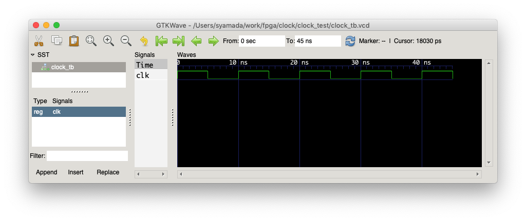
5ns ごとに,high と low が切り替わっていて,50ns でシミュレーションが終わっていることを確認しよう.
プロセス文の前のコロン
ちなみに,プロセス分の前のコロンは,オプションであってもなくてもよい.process 文の基本構成は,
process_optionlabel : process(sensitivity_list)
-- 宣言部
begin
-- 順次処理
end process process_optionlabel;
である.ただし,VHDL Process Statement にあるように,コードの可読性やシミュレーション時に便利らしいので,使うことも多いようである.
clock の分周方法
次に,クロックの分周について練習してみよう.
コード
クロックの分周とは,一つのクロックを用いて,タイミングの異なるクロックを生成することで,方法だけでなく,タイミング制約やリソースの事など気をつけることが色々とあるようでだが,ここでは,How To Implement Clock Divider in VHDLを参考に,クロックの分周について,練習してみよう.
library ieee;
use ieee.std_logic_1164.all;
use ieee.numeric_std.all;

entity clockdiv_tb is
end entity;

architecture sim of clockdiv_tb is

    constant ClockFrequency : integer := 100e6; -- 100 MHz
    constant ClockPeriod    : time    := 1000 ms / ClockFrequency;
    signal Clk : std_logic := '1';

    signal clk_divider : unsigned(2 downto 0) := (others=>'0');
    signal o_clk_div2 : std_logic :='0';
    signal o_clk_div4 : std_logic :='0';
    signal o_clk_div8 : std_logic :='0';
    signal rst : std_logic :='0';

begin
    -- Process for generating the clock
    Clk <= not Clk after ClockPeriod / 2;

    -- Clock Divider Counter
    p_clk_divider: process(rst,Clk)
    begin
    if(rst='0') then
        clk_divider   <= (others=>'0');
      elsif(rising_edge(Clk)) then
        clk_divider   <= clk_divider + 1;
     end if;
    end process p_clk_divider;

    o_clk_div2    <= clk_divider(0);
    o_clk_div4    <= clk_divider(1);
    o_clk_div8    <= clk_divider(2);

    -- Testbench sequence
    clktest: process is
    begin
    	wait for 20 ns;
        rst <= '1';
        wait for 400 ns;
        assert (false) report "Simulation End!" severity failure;
        wait;
    end process clktest;

end architecture;
clk_divider というカウンターを + 1 し続けるだけである.ただし,
unsigned(2 downto 0) とは,3ビットあり,それを超えて + 1 されると 0 に戻ることを使っている.つまり,111 に +1 すると,000 に戻る.このビットを使うかを o_clk_div2,o_clk_div4, o_clk_div8 が待ち構えている.
シミュレーション結果
コンパイルは,先ほどと同じで,
ghdl -a --ieee=synopsys clockdiv_tb.vhd
ghdl -e --ieee=synopsys clockdiv_tb
ghdl -r --ieee=synopsys clockdiv_tb --vcd=clockdiv_tb.vcd
とする.
その結果は,
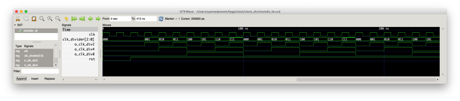
のようになり,元の100MHzのクロックが,1/2, 1/4, 1/8とされていることがわかる.
プロセス文 : signal と variable の挙動の違い
プロセス文は順次処理と呼ばれるが,singal と variable の挙動の違いはソフトウェアのコーディングのイメージだと間違えてしまうので,確実に理解しておきたい.
コード
サンプルコードは,VHDLの基本を忘れてしまった python ユーザーの備忘録 の "Process文って何だっけ." を確認できる格好にした.
library ieee;
use ieee.std_logic_1164.all;
use ieee.numeric_std.all;

entity proc_tb is
end entity;

architecture sim of proc_tb is

    constant ClockFrequency : integer := 100e6; -- 100 MHz
    constant ClockPeriod    : time    := 1000 ms / ClockFrequency;
    signal Clk : std_logic := '1';

    signal a : integer := 1;
    signal b : integer := 2;
    signal c : integer := 10;
    signal d : integer := 4;
    signal x : integer := 0;
    signal y : integer := 0;

begin
    -- Process for generating the clock
    Clk <= not Clk after ClockPeriod / 2;

    -- Testbench sequence
    process is
    variable v : integer :=0;

    begin
    	wait for 20 ns;
    	a <= a + b;
    	wait for 20 ns;
    	d <= a;
    	wait for 20 ns;
    	d <= a;
    	x <= b + d; -- add signal d
    	d <= c;
    	y <= b + d; -- add signal d
    	wait for 20 ns;
    	v := a;
    	x <= b + v; -- add variable v
    	v := c;
    	y <= b + v; -- add variable v
    	wait for 20 ns;


        assert (false) report "Simulation End!" severity failure;
        wait;
    end process;

end architecture;
確認事項
b + d(signal) と b + v(variable) を2回やるパターンで,その前後に,
d(signal) または v(variable) が更新されているときに,答えがどうなるかを確認しよう.
答えは,signal の場合は,評価(最後の演算)が行われた後に,代入が行われるので,x <= b + d と y <= b + d の結果はどちらも,d <= c が加算されるので同じになるのに対して,variable を使った場合は直前の値が使われるので値が異なる.
シミュレーション結果
コンパイルは同様に,
ghdl -a --ieee=synopsys proc_tb.vhd
ghdl -e --ieee=synopsys proc_tb
ghdl -r --ieee=synopsys proc_tb --vcd=proc_tb.vcd
として,結果はこのようになる.
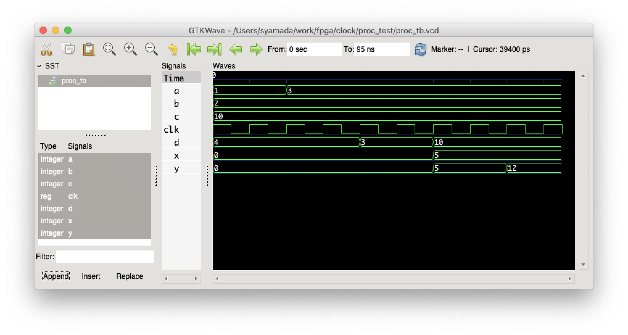
最後の20nsで,y の値が更新されていることがわかるだろう.
もっともシンプルな例
イマイチな説明でわかりにくかったかもしれないので,超簡単な例も紹介しておきます.
library ieee;
use ieee.std_logic_1164.all;
use ieee.numeric_std.all;

entity procsimple_tb is
end entity;

architecture sim of procsimple_tb is

    constant ClockFrequency : integer := 100e6; -- 100 MHz
    constant ClockPeriod    : time    := 1000 ms / ClockFrequency;
    signal Clk : std_logic := '1';

    signal a : integer := 1;
    signal b : integer := 2;
    signal c : integer := 100;

begin
    -- Process for generating the clock
    Clk <= not Clk after ClockPeriod / 2;

    -- Testbench sequence
    process is
    begin
    	wait for 20 ns;
    	a <= b;
        a <= c;
    	wait for 20 ns;
        assert (false) report "Simulation End!" severity failure;
    end process;

end architecture;
これを実行すると,
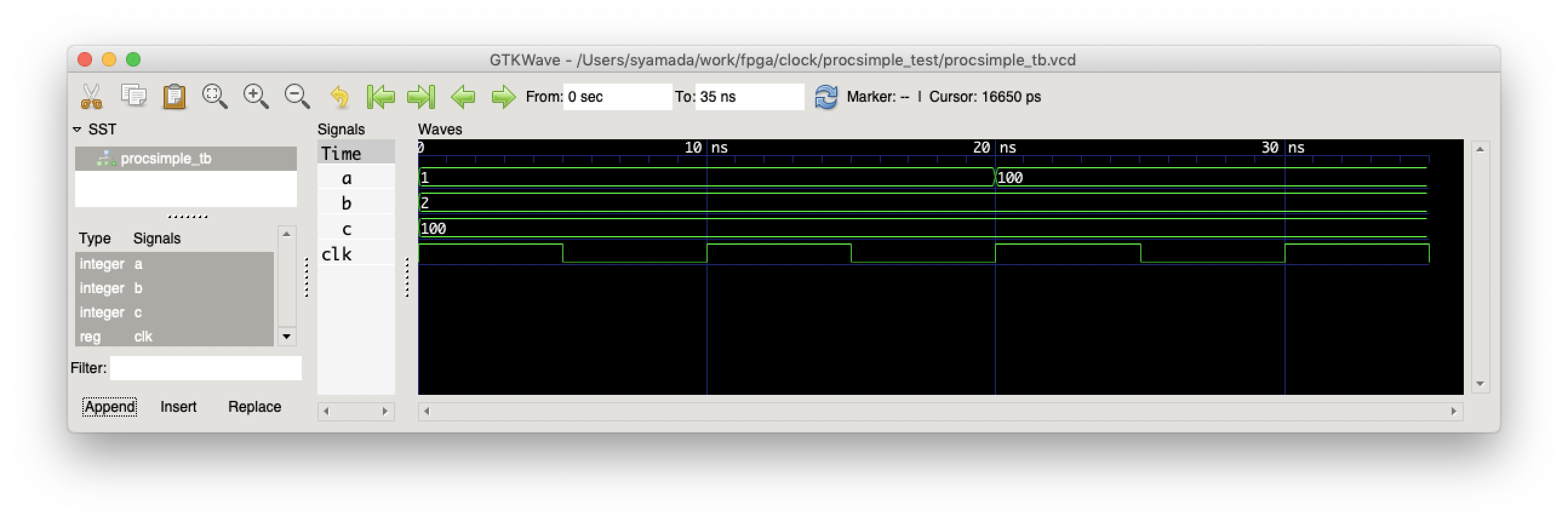
このようになり,a は,100(つまりbではなく,c)になっている.つまり,signal の場合は,最後に評価された値になるのが,日本語の"順次処理"の連想から外れるところであり,pythonやCなどのソフトウェアと感覚的に違い,間違いやすいところである.
フリップフロップ
ここでは,HOW TO CREATE A CLOCKED PROCESS IN VHDL で Jonas さんの記事を読むのが一番であるが,日本語で少し噛み砕いて紹介しておきたい.
そもそも,フリップフロップって何?という人向けに少し説明しておきます.FPGAの開発のどこで使うか?という以前に,FPGAの基本構造である「ロジックセル」は、「ルックアップテーブル」(Look Up Table:LUT)と「フリップフロップ」(Flip Flop)の2つから構成されるので,FPGA自体が Flip Flop の集合体のようなものです.いまさら聞けない FPGA入門 など参照.
フリップフロップの役割は,例えばこう考えてみるとどうだろうか.ある回路を自作したとして,入力信号に依存して任意の信号が出力されるものを作ったとしよう.この時に,入力信号が取り去られると,出力は全て忘れて初めの状態に戻ってしまうとどうなるだろうか.パルスを連続的に発生させるような場合はそれでよいかもしれないが,後段に情報を受け渡したいときにはそれだと困ってしまうだろう.フリップフロップ回路は,入力信号を取り去っても,その出力状態を維持し続けることができる.このため,フリップフロップ回路は,ラッチ(留め金という意味)回路とも呼ばれ,1ビット情報を保持(記憶)することができる回路としてよく使われる.
コード
ff.vhd には,フリップフロップの中身が書かれていて,ff_tb.vhd はそれを用いてテストするためのコードである.
library ieee;
use ieee.std_logic_1164.all;
use ieee.numeric_std.all;

entity ff is
port(
    Clk    : in std_logic;
    nRst   : in std_logic; -- Negative reset
    Input  : in std_logic;
    Output : out std_logic);
end entity;

architecture rtl of ff is
begin

    -- Flip-flop with synchronized reset
    process(Clk) is
    begin
        if rising_edge(Clk) then
            if nRst = '0' then
                Output <= '0';
            else
                Output <= Input;
            end if;
        end if;
    end process;

end architecture;
library ieee;
use ieee.std_logic_1164.all;
use ieee.numeric_std.all;

entity ff_tb is
end entity;

architecture sim of ff_tb is

    constant ClockFrequency : integer := 100e6; -- 100 MHz
    constant ClockPeriod    : time    := 1000 ms / ClockFrequency;

    signal Clk : std_logic := '1';
    signal nRst : std_logic := '0';
    signal Input : std_logic := '0';
    signal Output : std_logic;

begin

    -- The Device Under Test (DUT)
    i_ff : entity work.ff(rtl)
    port map(
        Clk    => Clk,
        nRst   => nRst,
        Input  => Input,
        Output => Output);

    -- Process for generating the clock
    Clk <= not Clk after ClockPeriod / 2;

    -- Testbench sequence
    process is
    begin
        -- Take the DUT out of reset
        nRst <= '1';

        wait for 18 ns;
        Input <= '1';
        wait for 18 ns;
        Input <= '0';
        wait for 6 ns;
        Input <= '1';
        wait for 28 ns;
        Input <= '0';
        wait for 13 ns;
        Input <= '1';
        wait for 23 ns;
        -- Reset the DUT
        nRst <= '0';
        wait for 20 ns;

        assert (false) report "Simulation End!" severity failure;
        wait;
    end process;
end architecture;
シミュレーション結果
コンパイルは
ghdl -a --ieee=synopsys ff.vhd
ghdl -a --ieee=synopsys ff_tb.vhd
ghdl -e --ieee=synopsys ff_tb
ghdl -r --ieee=synopsys ff_tb --vcd=ff_tb.vcd
のように,-a オプションで実行するのが一つ増えただけである.
シミュレーション結果はこのようになる.
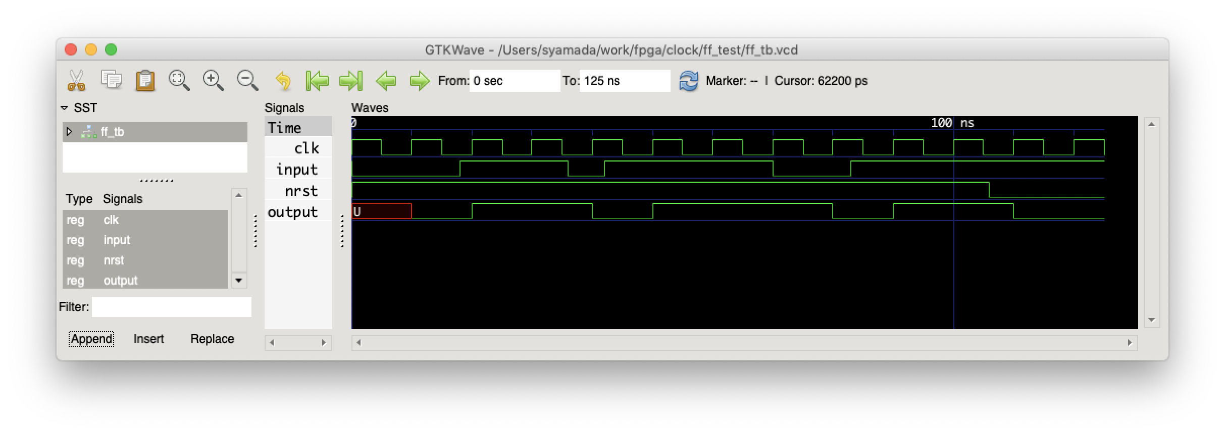
Input が 1 の間に,clk の立ち上がりが来た時だけ,output が値をラッチして 1に代わり,Input が 0 の間に,clk の立ち上がりが来ると,output が 0 に変化する.また,nrst が 0 になると,output が 0 に初期化される.
リングバッファ (ring/circular buffer)
リングバッファ,あるいは,circuclar buffer は,循環型のメモリで,wikipedia の英語版の説明 circular buffer が動画もあってよくまとまっている.
これをFPGAで実装するには良い例が昔はなかったのであるが,https://vhdlwhiz.com が物凄くわかりやすくまとめてくれていて,超参考になる.https://vhdlwhiz.com/ring-buffer-fifo/ を読むことを一番推奨するが,ここでは,少し補足説明しつつ,gtkwave でシミュレーションが動くところまで丁寧に説明してみる.
コード
vhdlwhiz.comのring-buffer-fifo を用いて説明する.
大きなパートは
- PROC_HEAD : リングバッファの書き込みポインタ(head)を更新するプロセス
- PROC_TAIL : リングバッファの読み出しポインタ(tail)を更新するプロセス
- PROC_RAM : RAM の head 部分に書き込み,tail 部分を読み出す
- PROC_COUNT : 保存しているデータ数を更新する.ただし,head が一番後ろまで達して,最初の戻ると,head の方が tail より小さくなるので,その場合分けをして計算する.
の4つのプロセスから構成される.
そのほか,あるクロックでRAMが満杯になった時に,その次のクロックで書き込まない,あるいは,その次を読み出さないために,満杯になる1clock前の状態と空になる1clock前の状態を検知できるようにしている.それらが,full_next,empty_next という出力である.
library ieee;
use ieee.std_logic_1164.all;

entity ring_buffer is
  generic (
    RAM_WIDTH : natural;
    RAM_DEPTH : natural;
  );
  port (
    clk : in std_logic;
    rst : in std_logic;

    -- Write port
    wr_en : in std_logic;
    wr_data : in std_logic_vector(RAM_WIDTH - 1 downto 0);

    -- Read port
    rd_en : in std_logic;
    rd_valid : out std_logic;
    rd_data : out std_logic_vector(RAM_WIDTH - 1 downto 0);

    -- Flags
    empty : out std_logic;
    empty_next : out std_logic; -- 次の1clockで空になると教えてくれるフラグ
    full : out std_logic;
    full_next : out std_logic; -- 次の1clockでfullになると教えてくれるフラグ

    -- The number of elements in the FIFO
    fill_count : out integer range RAM_DEPTH - 1 downto 0
  );
end ring_buffer;

architecture rtl of ring_buffer is

  type ram_type is array (0 to RAM_DEPTH - 1) of std_logic_vector(wr_data'range);
  signal ram : ram_type;

  subtype index_type is integer range ram_type'range;
  signal head : index_type;
  signal tail : index_type;

  signal empty_i : std_logic;
  signal full_i : std_logic;
  signal fill_count_i : integer range RAM_DEPTH - 1 downto 0;

  -- Increment and wrap
  procedure incr(signal index : inout index_type) is
  begin
    if index = index_type'high then
      index <= index_type'low;
    else
      index <= index + 1;
    end if;
  end procedure;

begin

  -- Copy internal signals to output
  empty <= empty_i;
  full <= full_i;
  fill_count <= fill_count_i;

  -- Set the flags
  empty_i <= '1' when fill_count_i = 0 else '0';
  empty_next <= '1' when fill_count_i <= 1 else '0';
  full_i <= '1' when fill_count_i >= RAM_DEPTH - 1 else '0';
  full_next <= '1' when fill_count_i >= RAM_DEPTH - 2 else '0';

  -- Update the head pointer in write
  PROC_HEAD : process(clk)
  begin
    if rising_edge(clk) then
      if rst = '1' then
        head <= 0;
      else

        if wr_en = '1' and full_i = '0' then
          incr(head);
        end if;

      end if;
    end if;
  end process;

  -- Update the tail pointer on read and pulse valid
  PROC_TAIL : process(clk)
  begin
    if rising_edge(clk) then
      if rst = '1' then
        tail <= 0;
        rd_valid <= '0';
      else
        rd_valid <= '0';

        if rd_en = '1' and empty_i = '0' then
          incr(tail);
          rd_valid <= '1';
        end if;

      end if;
    end if;
  end process;

  -- Write to and read from the RAM
  PROC_RAM : process(clk)
  begin
    if rising_edge(clk) then
      ram(head) <= wr_data;
      rd_data <= ram(tail);
    end if;
  end process;

  -- Update the fill count
  PROC_COUNT : process(head, tail)
  begin
    if head < tail then
      fill_count_i <= head - tail + RAM_DEPTH;
    else
      fill_count_i <= head - tail;
    end if;
  end process;

end architecture;
これを動かすための,testbenchのスクリプトは下記である.
PROC_SEQUENCERの中で,
- 10 clock 分まってからリセットする
- クロックの立ち上がりを待って,wr_en <= '1' 書き込み可にする
- fifoがフルになるまで,wr_data <= std_logic_vector(unsigned(wr_data) + 1); で +1 したデータを生成する.
- wr_en <= '0' 書き込み不可にする
- rd_en <= '1' 読み出し可にする
という順番でデータを動かしている.
library ieee;
use ieee.std_logic_1164.all;
use ieee.numeric_std.all;

use std.env.finish;

entity ring_buffer_tb is
end ring_buffer_tb;

architecture sim of ring_buffer_tb is

  constant clock_period : time := 10 ns;

  -- Generics
  constant RAM_WIDTH : natural := 16;
  constant RAM_DEPTH : natural := 256;

  -- DUT signals
  signal clk : std_logic := '1';
  signal rst : std_logic := '1';
  signal wr_en : std_logic := '0';
  signal wr_data : std_logic_vector(RAM_WIDTH - 1 downto 0) := (others => '0');
  signal rd_en : std_logic := '0';
  signal rd_valid : std_logic;
  signal rd_data : std_logic_vector(RAM_WIDTH - 1 downto 0);
  signal empty : std_logic;
  signal empty_next : std_logic;
  signal full : std_logic;
  signal full_next : std_logic;
  signal fill_count : integer range RAM_DEPTH - 1 downto 0;

begin

  DUT : entity work.ring_buffer(rtl)
    generic map (
      RAM_WIDTH => RAM_WIDTH,
      RAM_DEPTH => RAM_DEPTH
    )
    port map (
      clk => clk,
      rst => rst,
      wr_en => wr_en,
      wr_data => wr_data,
      rd_en => rd_en,
      rd_valid => rd_valid,
      rd_data => rd_data,
      empty => empty,
      empty_next => empty_next,
      full => full,
      full_next => full_next,
      fill_count => fill_count
    );

    clk <= not clk after clock_period / 2;

    PROC_SEQUENCER : process
    begin

      wait for 10 * clock_period;
      rst <= '0';
      wait until rising_edge(clk);

      -- Start writing
      wr_en <= '1';

      -- Fill the FIFO
      while full_next = '0' loop
        wr_data <= std_logic_vector(unsigned(wr_data) + 1);
        wait until rising_edge(clk);
      end loop;

      -- Stop writing
      wr_en <= '0';

      -- Empty the FIFO
      rd_en <= '1';
      wait until empty_next = '1';

      wait for 10 * clock_period;
      finish;
    end process;

end architecture;
シミュレーション結果
コマンドはいつも同じ出るが,finish文は,VHDL2008なので,--std=08 をオプションにつける.
ghdl -a --ieee=synopsys --std=08 ring_buffer.vhd
ghdl -a --ieee=synopsys --std=08 ring_buffer_tb.vhd
ghdl -e --ieee=synopsys --std=08 ring_buffer_tb
ghdl -r --ieee=synopsys --std=08 ring_buffer_tb --vcd=ring_buffer_tb.vcd
gtkwave で波形を確認すると,
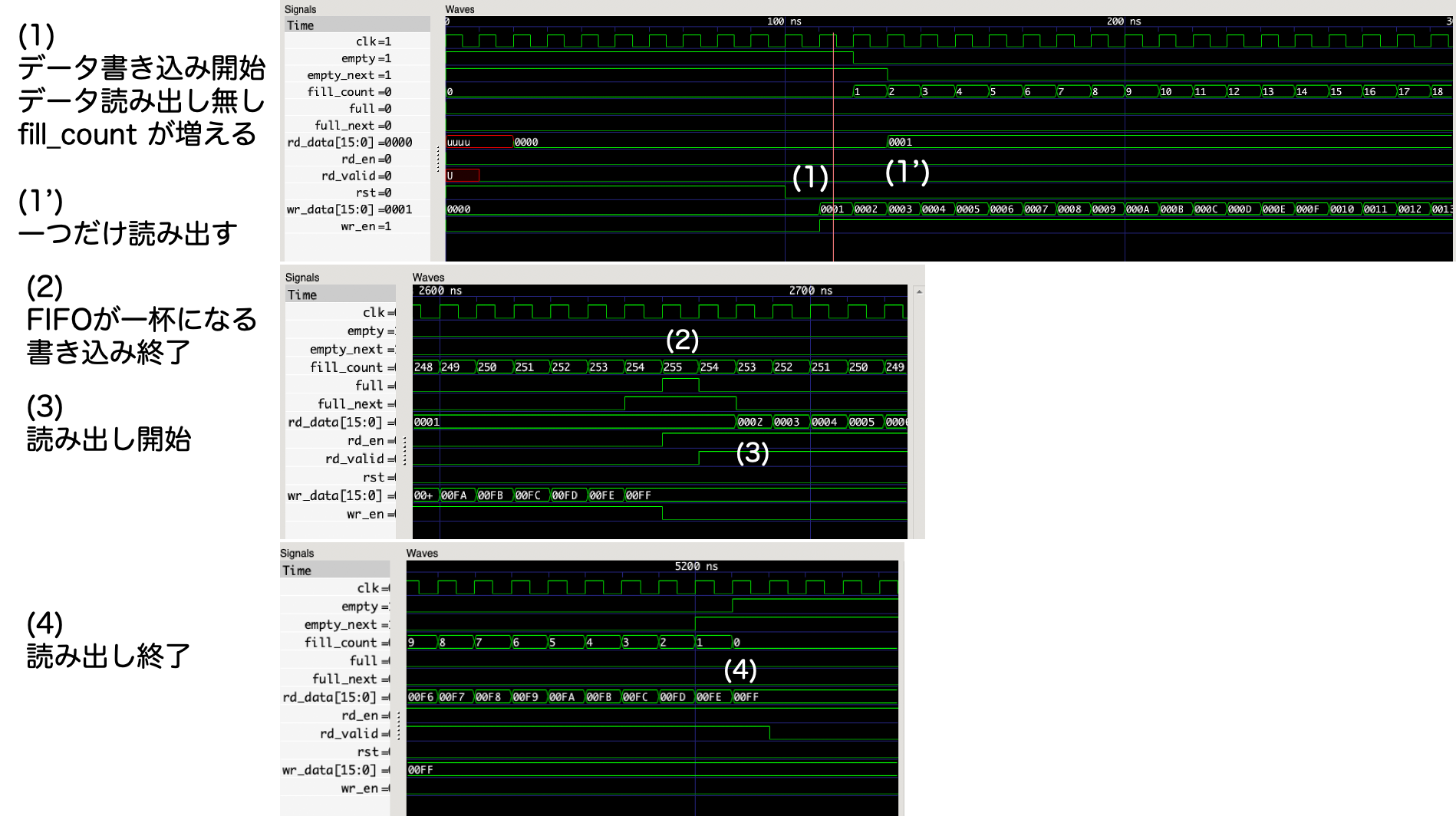
のように見える.