最近良くAliexpressで見かける表面実装はんだ付け基板を買ってみました。

ただの練習用基板ではなく、完成したら何かが動くような気がしたので、販売しているショップのいくつかに
「回路図が有ったら展開してください」とメールを送ったら日膣の店舗から回路図をいただきました。
回路図を送ってくれた店舗はこちらのショップになります。
https://ja.aliexpress.com/item/1005002012033537.html
回路図はこれです。
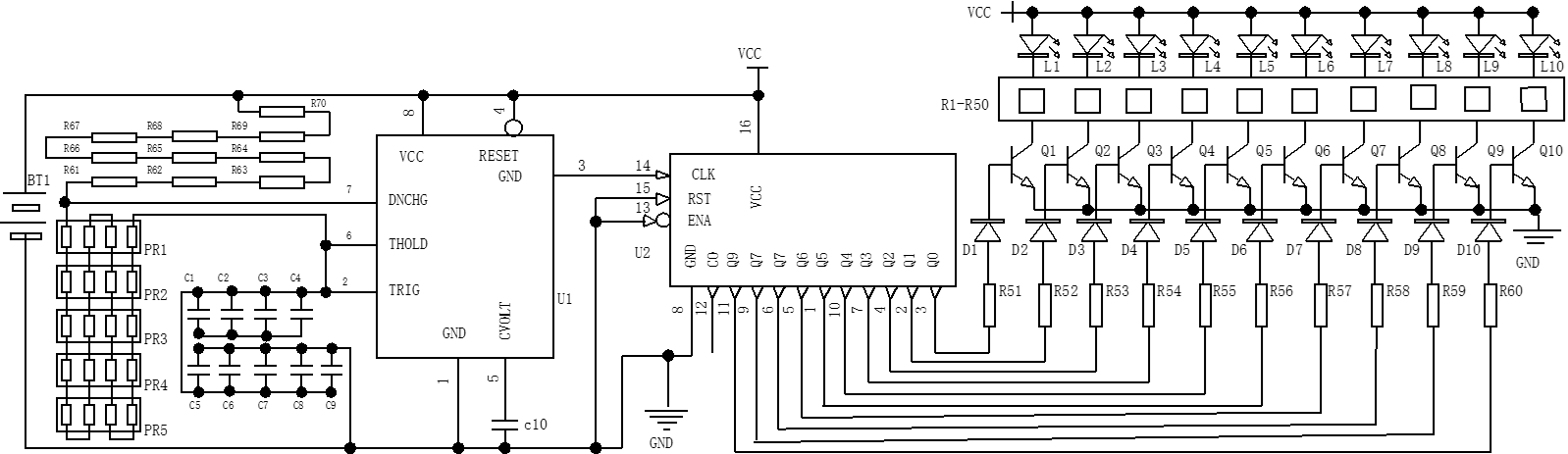
部品表です

QFP44のIC2個は使っていないみたいで、ただ単にはんだ付けの練習用でしょう。
回路の概要
タイマーIC(555)でクロック信号を発生させて、
10 デコード出力、CMOS 10 進カウンタ IC CD4017BでLEDを順次点灯する回路ですね。
CD4017Bでは直接LEDを点灯することが出来ないので
LEDのドライブ用として Q1~Q10のトランジスタを使っています。
トランジスタの型式は不明ですが一般的なNPNトランジスタ、
例えば秋月電子で売られている40個200円の2SC2712-GRあたりかと思います。
秋月電子 SC2712-GR
CD4017Bデータシート
LM555データシート
回路図と一緒に頂いた説明書の原本と自動翻訳の日本語を掲載しておきます。
英語の原本
1, Soldering the Component Welding Practice Board.
2, Electrify it and it will form flowing water light, then test the soldering effect.
3, When the power is turned on, the voltage on both ends of the capacitors C1-C9 cannot be changed abruptly. The pin 2 of NE555 is at a low level and the output pin 3 is at a high level.
4, When power supply charged from R61-R70 and RP1-PR5 to C1-C9 till 2/3 power supply voltage, the output pin 3 electrical level will changes from high to low, NE555 internal guide on, the capacitors
C1-C9 are discharged through pin 7 of 555 until the voltage across C1-C9 is less than 1/3 of the power supply voltage, pin 3 of 555 electrical level will changes from low level to high level again,
C1-C9 charges again, then it will forms a cyclic shock.
5, Change the size of RP1-RP5 can change the output frequency of the oscillator. The 555 clock oscillation signal is continuously added to pin 14 of 4017, 10 output terminals of 4017 are connected with
10 transistors to drive 10 LEDs, 10 output terminals of 4017 are produced high level in turn under the action of clock signal. Then the L1-L10 are lighted at a time, forming the effect of a beautiful water lamp circuit.
Parameter:
Power supply voltage: DC 3V-5V
Precautions for welding: SMD components are relatively small, be careful not to lose
Attention:
The side of LED two lights with the green dot is the negative pole, when the power supply is powered, the positive pole is connected to +, and the negative pole is connected to negative-
Please contact us to get the PDF English Manual if necessary. Our email: melifeus@hotmail.com
DeepLでの日本語約
1、部品溶接練習用ボードをはんだ付けする。
2、通電して流水灯を形成し、ハンダ付け効果をテストする。
3, 電源投入時、コンデンサC1-C9の両端電圧を急激に変化させない。NE555の2番ピンはLowレベル、出力3番ピンはHighレベルになります。
4, R61-R70とRP1-PR5からC1-C9に電源電圧を2/3まで充電すると、出力端子3の電気レベルがHighからLowに変化し、NE555内部がガイドオンし、コンデンサC1-C9は放電され、出力端子3の電気レベルがHighになります。
C1-C9は、C1-C9間の電圧が電源電圧の1/3未満になるまで555のピン7を介して放電され、555のピン3はローレベルから再びハイレベルに変化します。
C1-C9 は再び充電し、周期的な衝撃を形成します。
5、RP1-RP5の大きさを変更すると、発振器の出力周波数を変更することができます。4017の14番ピンに555クロックの発振信号を連続的に加え、4017の出力端子10個をトランジスタ10個で接続し、10個のLEDを駆動します。
10個のLEDを駆動するために10個のトランジスタを接続し、クロック信号の作用で4017の10個の出力端子を順番にハイレベルにします。そして、L1-L10が一度に点灯し、美しい水ランプ回路の効果を形成します。
パラメータ
電源電圧。DC 3V-5V
溶接のための注意事項 SMD部品は比較的小さいので、紛失しないように注意してください。
注意してください。
LED2灯の緑色の点がある側がマイナス極で、電源投入時、プラス極は+に、マイナス極は-に接続されます。
この基板を製作しているところは近日中にYouTubeにアップします。