dsPIC33EV256GM102
修正 25.06.13 コンフィグレーションビットのデバッグ指定をPGD1からPGD3に変更。
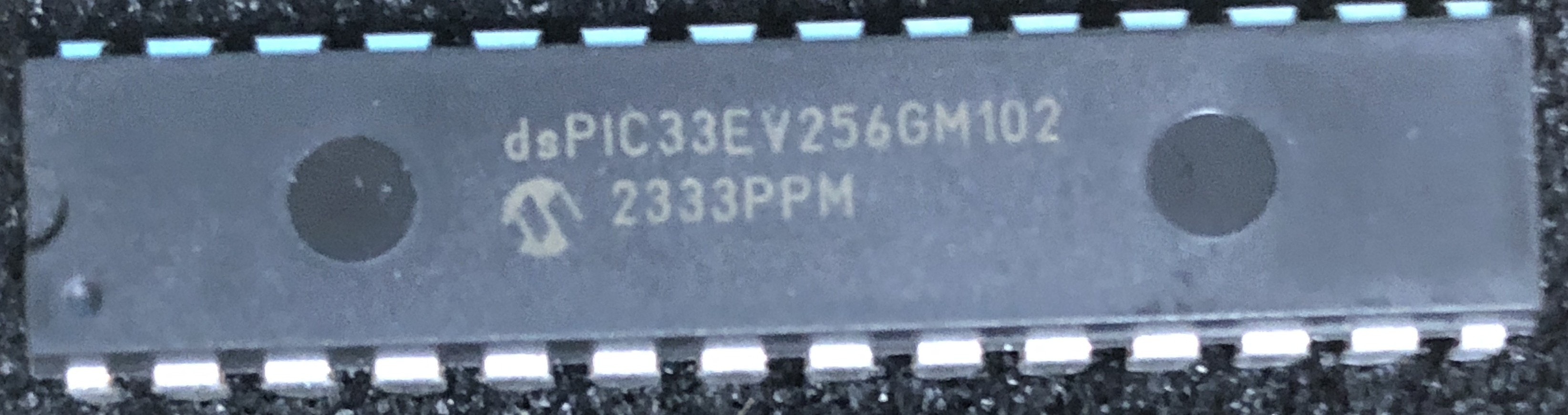
秋月電子通商で、今年の1月から新たに販売されたdsPIC。
・電源電圧が5Vオンリー、(なので、新たに基盤を組みました。)
※久しぶりに動かすとき、VDD=3.3Vにしないように。
・端子配列は、他のdsPICと同じ。
・書き込み線は、4番ピンSDA線、5番:SCL線にしました。


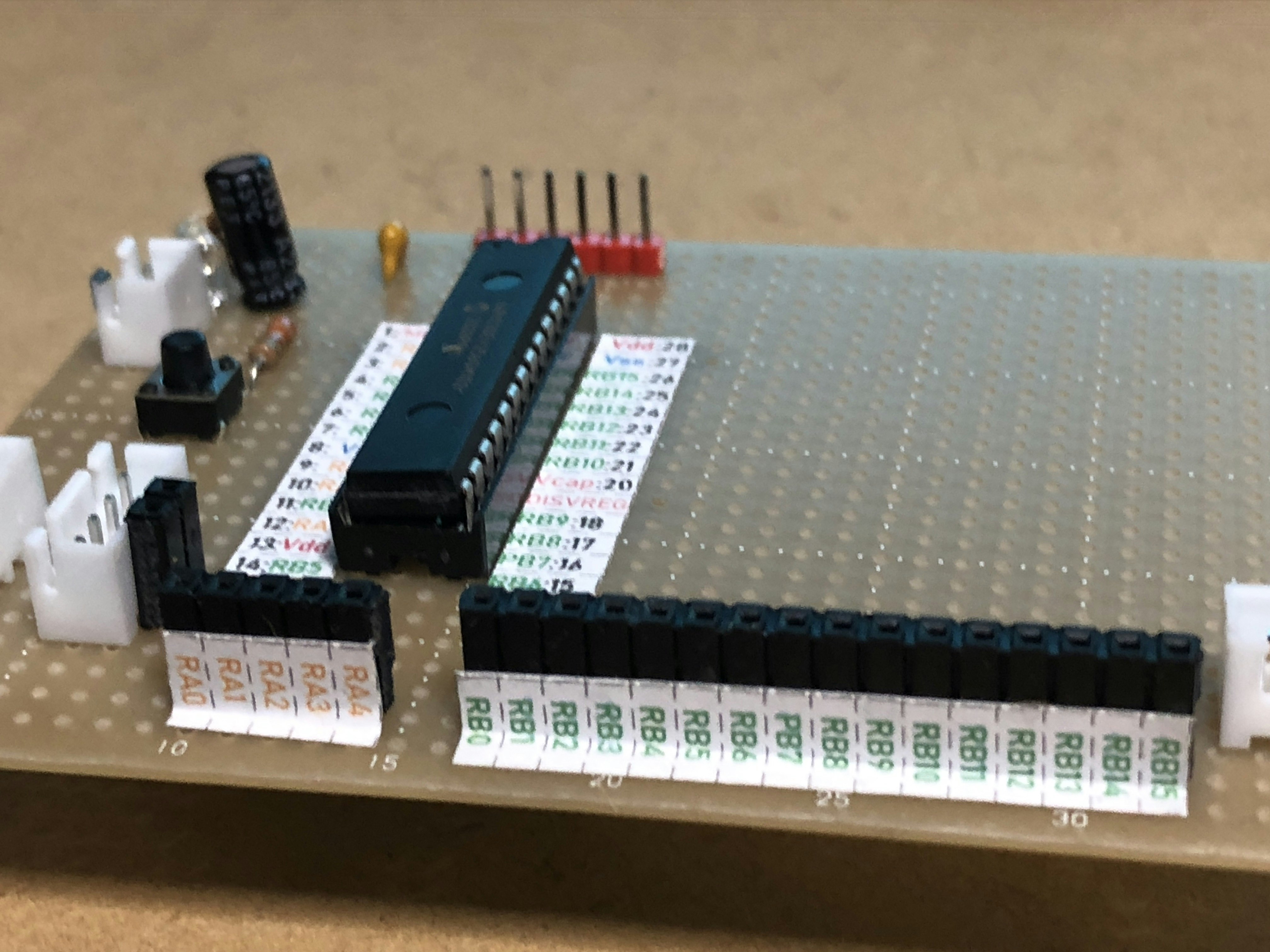
ピンソケットは、秋月の分割ロングピンソケット を使用しました。
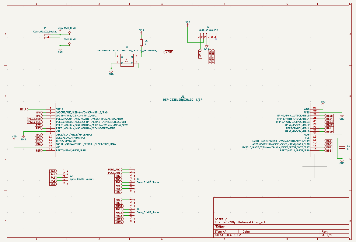
回路図
dsPIC33EV256GM102 Lチカコード
オシレータ設定のコードは、dsPIC33FJ、dsPIC33EPと同じです。
main.c
/*
 * File:   mainXC16.c
 * Created on 2025/06/05
 */

//#define FOSC 99495000//Mhz
#define FOSC 100000000UL//Mhz Fosc System clock
#define FCY  FOSC/2 //instruction clock frequency libpic30.hより前で宣言すること
#include "xc.h"
#include "ds_peripheral.h"

//*************************************************
// DSPIC33EV256GM102 Configuration Bit Settings
//*************************************************

// 'C' source line config statements

#include <p33Exxxx.h>
#include <libpic30.h>

// FSEC
#pragma config BWRP = OFF               // Boot Segment Write-Protect Bit (Boot Segment may be written)
#pragma config BSS = DISABLED           // Boot Segment Code-Protect Level bits (No Protection (other than BWRP))
#pragma config BSS2 = OFF               // Boot Segment Control Bit (No Boot Segment)
#pragma config GWRP = OFF               // General Segment Write-Protect Bit (General Segment may be written)
#pragma config GSS = DISABLED           // General Segment Code-Protect Level bits (No Protection (other than GWRP))
#pragma config CWRP = OFF               // Configuration Segment Write-Protect Bit (Configuration Segment may be written)
#pragma config CSS = DISABLED           // Configuration Segment Code-Protect Level bits (No Protection (other than CWRP))
#pragma config AIVTDIS = DISABLE        // Alternate Interrupt Vector Table Disable Bit  (Disable Alternate Vector Table)

// FBSLIM
#pragma config BSLIM = 0x1FFF           // Boot Segment Code Flash Page Address Limit Bits (Enter Hexadecimal value)

// FOSCSEL
#pragma config FNOSC = FRCDIVN          // Initial oscillator Source Selection Bits (Internal Fast RC (FRC) Oscillator with postscaler)
#pragma config IESO = ON                // Two Speed Oscillator Start-Up Bit (Start up device with FRC,then automatically switch to user selected oscillator source)

// FOSC
#pragma config POSCMD = NONE            // Primary Oscillator Mode Select Bits (Primary Oscillator disabled)
#pragma config OSCIOFNC = OFF           // OSC2 Pin I/O Function Enable Bit (OSC2 is clock output)
#pragma config IOL1WAY = OFF            // Peripheral Pin Select Configuration Bit (Allow Multiple reconfigurations)
#pragma config FCKSM = CSECMD           // Clock Switching Mode Bits (Clock Switching is enabled,Fail-safe Clock Monitor is disabled)
#pragma config PLLKEN = ON              // PLL Lock Enable Bit (Clock switch to PLL source will wait until the PLL lock signal is valid)

// FWDT
#pragma config WDTPOST = PS32768        // Watchdog Timer Postscaler Bits (1:32,768)
#pragma config WDTPRE = PR128           // Watchdog Timer Prescaler Bit (1:128)
#pragma config FWDTEN = OFF             // Watchdog Timer Enable Bits (WDT and SWDTEN Disabled)
#pragma config WINDIS = OFF             // Watchdog Timer Window Enable Bit (Watchdog timer in Non-Window Mode)
#pragma config WDTWIN = WIN25           // Watchdog Window Select Bits (WDT Window is 25% of WDT period)

// FPOR
#pragma config BOREN0 = ON              // Brown Out Reset Detection Bit (BOR is Enabled)

// FICD
#pragma config ICS = PGD3               // ICD Communication Channel Select Bits (Communicate on PGEC3 and PGED3)

// FDMTINTVL
#pragma config DMTIVTL = 0xFFFF         // Lower 16 Bits of 32 Bit DMT Window Interval (Enter Hexadecimal value)

// FDMTINTVH
#pragma config DMTIVTH = 0xFFFF         // Upper 16 Bits of 32 Bit DMT Window Interval (Enter Hexadecimal value)

// FDMTCNTL
#pragma config DMTCNTL = 0xFFFF         // Lower 16 Bits of 32 Bit DMT Instruction Count Time-Out Value (Enter Hexadecimal value)

// FDMTCNTH
#pragma config DMTCNTH = 0xFFFF         // Upper 16 Bits of 32 Bit DMT Instruction Count Time-Out Value (Enter Hexadecimal value)

// FDMT
#pragma config DMTEN = DISABLE          // Dead Man Timer Enable Bit (Dead Man Timer is Disabled and can be enabled by software)

// FDEVOPT
#pragma config PWMLOCK = OFF            // PWM Lock Enable Bit (PWM registers may be written without key sequence)
#pragma config ALTI2C1 = OFF            // Alternate I2C1 Pins Selection Bit (I2C1 mapped to SDA1/SCL1 pins)

// FALTREG
#pragma config CTXT1 = NONE             // Interrupt Priority Level (IPL) Selection Bits For Alternate Working Register Set 1 (Not Assigned)
#pragma config CTXT2 = NONE             // Interrupt Priority Level (IPL) Selection Bits For Alternate Working Register Set 2 (Not Assigned)

// #pragma config statements should precede project file includes.
// Use project enums instead of #define for ON and OFF.


//---------------------------------
//dsPIC初期化関数
// IO,オシレータ設定(100Mhz)
//---------------------------------
 void dsPicInit(void)
 {
    TRISA=0x0000;
    TRISB=0x0000;
    ANSELA=0x0000;
    ANSELB=0x0000;

    __delay_ms(1);
    /**
     * FRC=7.37kHz
     * FOSC=100Mhz
     * OSCTUNEでつじつま合わせ。計算上99.495MHzなので。
     */
    CLKDIVbits.FRCDIV=0b000;//(7.37MHz)
    CLKDIVbits.PLLPRE=0b00000;//N1=2
    CLKDIVbits.PLLPOST=0b00;//N2=2
    PLLFBD = 0x034;//M=52
    OSCTUN  = 0x0003; //100MHz微調整

   __builtin_write_OSCCONH(0x01);
   __builtin_write_OSCCONL(OSCCONL | 0x01);//OSCCONbits.OSWEN=1;
    while(OSCCONbits.COSC!=0b001);
    while(OSCCONbits.LOCK!=1);
 }


int main(void)
{
    dsPicInit();

    while(1)
    {
        LATAbits.LATA0=1;
        __delay_ms(500);
        LATAbits.LATA0=0;
        __delay_ms(500);
    }
    return 0;
}