はじめに
本記事では、
TiberCadのGmsh + ドリフト拡散モデルを用いて、MOSFET 構造の 2D デバイスシミュレーションを行う例を紹介します。
今回はTiberCadのexample 4の内容に基づいたシミュレーションについてご紹介いたします。
全体の流れ
本記事で扱う解析の流れは次の通りです。
Gmsh 形式(.geo)で MOSFET 断面構造を定義してメッシュ生成
↓
Physical Surface / Line を使って物理領域と端子を定義
↓
TiberCad の Device / Module 入力で材料・ドーピング・境界条件を設定
↓
ドリフト拡散モデルで電流・キャリア分布を解析
1. MOSFET の 2D 構造定義(.geo)
構造の概要
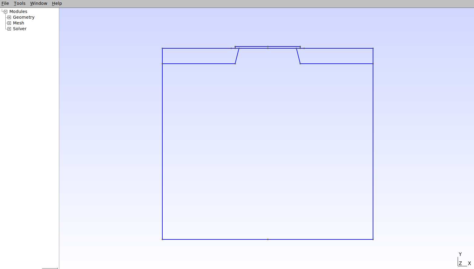
今回定義した構造は以下のような 2D 断面 MOS 構造です。
p型 Si 基板(substrate)
左右に n+ ドーピングされたソース / ドレイン領域(contact)
表面に SiO₂(oxide)
酸化膜上にゲート電極(gate)
基板底面に back contact
以下がmosfet.geoファイルのスクリプトになります。
lsub=0.03;
lacc=0.002;
lct=0.0005;
lg=0.0015;
lh=0.005;
lc=0.0005;

Lg_2 = 0.0375;
d = 0.01;
Ls = 0.1;
h = 0.25;
b = 0.0025;
o = 0.005;

xd = Lg_2 + d;
xd2 = Lg_2 + d / 2;
xmax = xd + Ls - d;

Point(1) = {0, -h, 0, lsub};
Point(2) = {0, 0, 0, lc};
Point(3) = {xmax,-h,0.0,lsub};
Point(4) = {-xmax,-h,0.0,lsub};
Point(5) = {xmax,0,0.0,lh};
Point(6) = {-xmax,0,0.0,lh};
Point(7) = {-xd,0,0.0,lct};
Point(8) = {-Lg_2 - o,0,0.0,lc};
Point(9) = {Lg_2 + o,0,0.0,lc};
Point(10) = {xd,0,0.0,lct};
Point(11) = {-Lg_2,0,0,lc};
Point(12) = {Lg_2,0,0,lc};
Point(13) = {xmax,-0.02,0,lh};
Point(14) = {-xmax,-0.02,0,lh};
Point(15) = {-xd2,-0.02,0.0,lacc};
Point(16) = {xd2,-0.02,0.0,lacc};
Point(17) = {-Lg_2 - o,b,0,lg};
Point(18) = {Lg_2 + o,b,0,lg};
Point(19) = {0, b, 0, lg};

Line(1) = {4,1};
Line(2) = {3,13};
Line(6) = {4,14};
Line(7) = {10,9};
Line(8) = {12,2};
Line(9) = {8,7};
Line(10) = {11,8};
Line(11) = {9,12};
Line(13) = {7,6};
Line(19) = {5,10};
Line(28) = {1,3};
Line(29) = {2,11};
Line(30) = {14,15};
Line(31) = {15,11};
Line(32) = {14,6};
Line(33) = {16,12};
Line(34) = {16,13};
Line(35) = {13,5};
Line(36) = {8,17};
Line(37) = {9,18};
Line(38) = {18,19};
Line(39) = {19,17};


Line Loop(40) = {28,2,-34,33,8,29,-31,-30,-6,1};
Plane Surface(41) = {40};
Line Loop(42) = {30,31,9,10,13,-32};
Plane Surface(47) = {42};
Line Loop(43) = {34,35,7,11,19,-33};
Plane Surface(44) = {43};
Line Loop(45) = {8,29,36,10,-39,-38,-37,11};
Plane Surface(46) = {45};

Physical Surface("substrate") = {41}; // n-Si
Physical Surface("contact") = {44,47}; // n+-Si
Physical Surface("oxide") = {46}; // SiO2
Physical Line("source") = {13}; // source
Physical Line("gate") = {39,38}; // gate
Physical Line("drain") = {19}; // drain
Physical Line("backcontact") = {1,28}; // drain
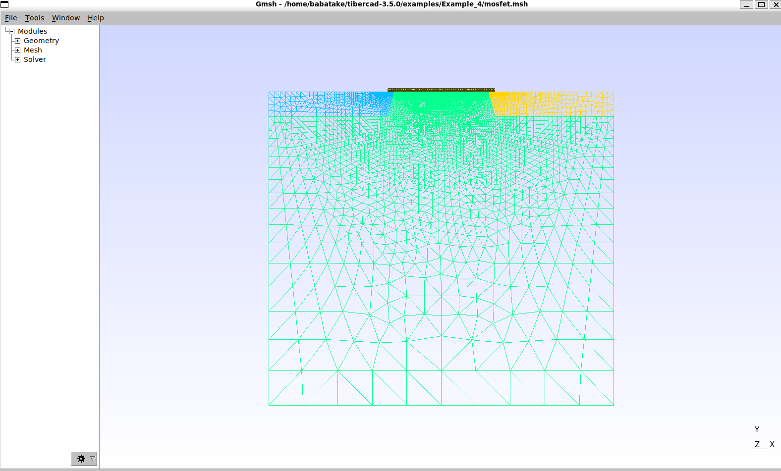
続いてこちらがgmshで表示させたデバイス断面とメッシュの画像です。
上の図のようにgmsh上で形状を作成したら、
gmshのmeshボタンをクリックするとメッシュ生成が行われます。
その後、メッシュファイルを保存します。
2. デバイス定義(Device ブロック)
次にmosfet.tibファイルを用いてデバイスの動作条件や使用するモデル(微分方程式)を設定していきます。
今回の事例ではある特定のゲート電圧(今回は1.0 V)を加えた時のI-Vカーブの取得のシミュレーションを実施します。
以下が、mosfet.tibのスクリプトです。
一見、自分でこのスクリプトを書くのはちょっと。。となりそうですが、
tibercadのマニュアルを生成AIに読み込ませて、それをもとに指示を与えれば、簡単に作成できます。
# Description of  the  device physical regions
Device mosfet
{
  meshfile = mosfet.msh
  write_boundary_mesh = true
  material = Si

  Region substrate
  {
    Doping
    {
      density = 1e18
      type = acceptor
    }
  }

  Region contact
  {
    Doping
    {
      density = 5e19
      type = donor
    }
  }

  Region oxide
  {
    material = SiO2
  }
}

# Definition of  Simulation Models  and associated Boundary Conditions
Module driftdiffusion
{
  plot = (Ec, Ev, eQFermi, eDensity, eCurrentDensity, eMobility,
          hQFermi, hDensity, hCurrentDensity, hMobility,
          NetRecombination, ElField, ElPotential, ContactCurrents)

  Solver
  {
    type = linesearch
    max_iterations = 20
    linear_solver
    {
      preconditioner = lu
    }
  }

  Physics
  {
    recombination srh {}
    mobility field_dependent
    {
      low_field_model = doping_dependent
    }
  }

  Contact gate
  {
    type = schottky
    barrier_height = 3.0

    # Vg をデフォルト 1.0V に固定(必要ならコマンドラインで上書き可能)
    voltage = $Vg[1.0]

    area_factor = 0.1
  }

  Contact source
  {
    voltage = 0.0
    area_factor = 0.1
  }

  Contact backcontact
  {
    voltage = 0.0
    area_factor = 0.1
  }

  Contact drain
  {
    # Vd を sweep するのでデフォルトは 0V
    voltage = $Vd[0.0]
    area_factor = 0.1
  }
}

# --- Drain I-V at fixed gate bias (Vg=1V) ---
Module sweep
{
  name     = sweep_drain
  solve    = driftdiffusion
  variable = $Vd
  start    = 0.0
  stop     = 2.0
  steps    = 40
  plot_data = true
}

Simulation
{
  solve = sweep_drain
  resultpath = output_outputchar_Vg1
  output_format = vtk
}
シミュレーションの実行
Example 4のフォルダに端末上で移動したら、
tibercad mosfet.tib
とすると、シミュレーションが始まります。
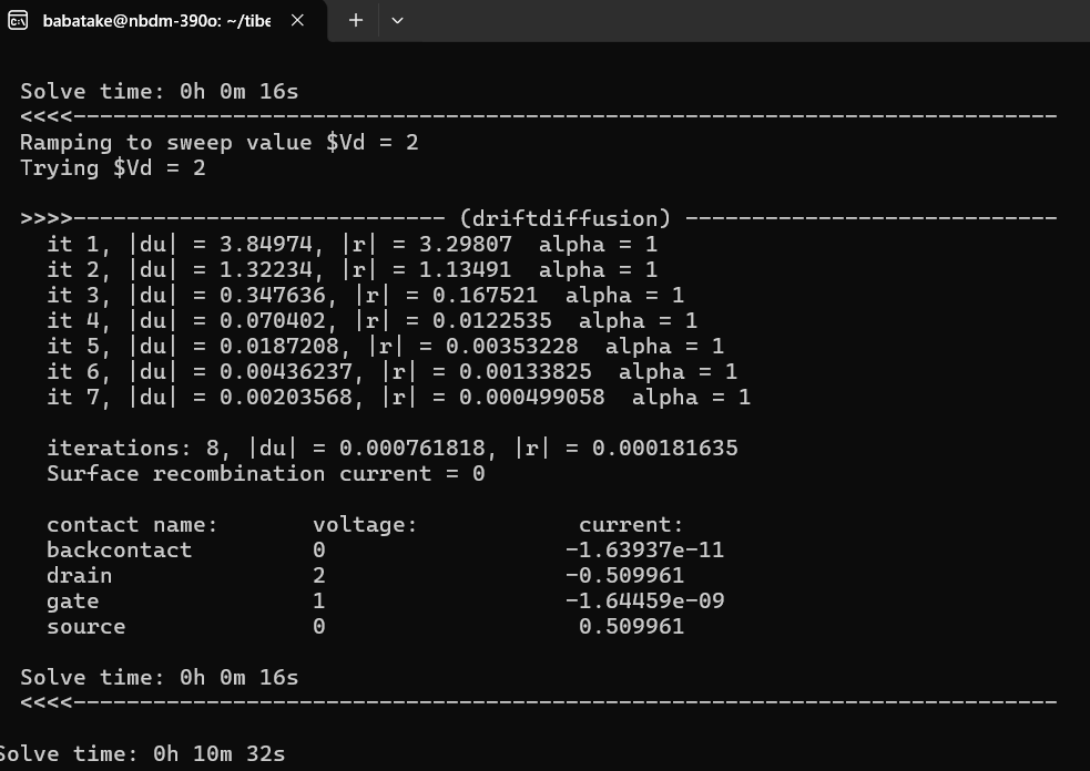
こちらが解析中のログ画面です。
解析結果
解析が終わると、sweep_drain_driftdiffusion.datファイルが出力されます。
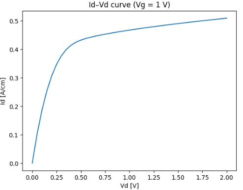
こちらがシミュレーション結果になります。トランジスタの動作として概ね傾向を再現していることがわかります。
*ただし、今回の計算ではゲート部分はMIS(Metal-Insulator-Semiconductor)ではなくショットキーに注意
今回はトランジスタを題材としてTiberCadの事例を紹介しました。TiberCadには量子井戸や量子井戸の利得解析機能もありますので、色々試してみると良いでしょう。
参考リンク
※本記事は筆者個人の見解であり、所属組織の公式見解を示すものではありません。
問い合わせ
光学シミュレーションソフトの導入や技術相談、
設計解析委託をお考えの方はサイバネットシステムにお問合せください。
光学ソリューションサイトについては以下の公式サイトを参照:
👉 光学ソリューションサイト(サイバネット)
光学分野のエンジニアリングサービスについては以下の公式サイトを参照:
👉 光学エンジニアリングサービス(サイバネット)