import numpy as np
import matplotlib.pyplot as plt
# 定数の設定 (Setting constants)
Vdd = 5.0 # 電源電圧 (Supply voltage)
V_Tn = 1.0 # NMOSのしきい値電圧 (Threshold voltage for NMOS)
V_Tp = -1.0 # PMOSのしきい値電圧 (Threshold voltage for PMOS)
# 定数の設定 (Setting constants for mobility and oxide capacitance)
mu_n = 600e-4 # NMOSの移動度 (Electron mobility for NMOS)
mu_p = 300e-4 # PMOSの移動度 (Hole mobility for PMOS)
C_ox = 3.45e-3 # 酸化膜容量 (Oxide capacitance)
# NMOSとPMOSのWとLを定義 (Define W and L for NMOS and PMOS)
W_n = 10e-6 # NMOSのチャンネル幅 (Channel width for NMOS)
L_n = 2e-6 # NMOSのチャンネル長 (Channel length for NMOS)
W_p = 20e-6 # PMOSのチャンネル幅 (Channel width for PMOS)
L_p = 2e-6 # PMOSのチャンネル長 (Channel length for PMOS)
# βnとβpの計算 (Calculate βn and βp)
beta_n = mu_n * C_ox * (W_n / L_n)
beta_p = mu_p * C_ox * (W_p / L_p)
# 計算結果を表示 (Display calculated values)
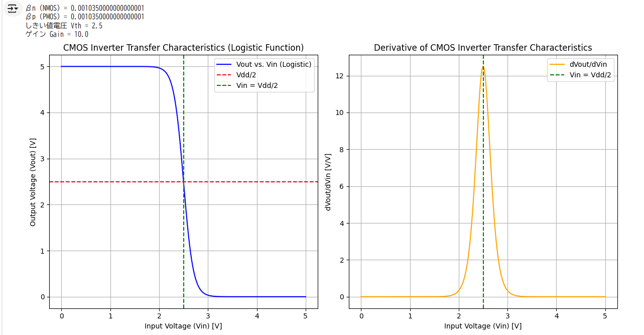
print(f"βn (NMOS) = {beta_n}")
print(f"βp (PMOS) = {beta_p}")
# しきい値電圧Vthの計算 (Calculate Vth based on the provided formula)
Vth = (Vdd + V_Tp + np.sqrt(beta_n / beta_p) * V_Tn) / (1 + np.sqrt(beta_n / beta_p))
# しきい値電圧を表示 (Display calculated Vth)
print(f"しきい値電圧 Vth = {Vth}")
# ゲインの計算 (Calculate gain using the provided formula)
gmp = 1e-3 # PMOS transconductance (S)
gmn = 1e-3 # NMOS transconductance (S)
rop = 10e3 # PMOS output resistance (ohms)
ron = 10e3 # NMOS output resistance (ohms)
gain = (gmp + gmn) / (1/rop + 1/ron)
# ゲインを表示 (Display calculated gain)
print(f"ゲイン Gain = {gain}")
# ロジスティック関数を使ったCMOSインバーターの出力 (CMOS inverter output using logistic function)
def logistic_inverter(Vin, Vdd, Vth, gain):
return Vdd * (1 / (1 + np.exp(-gain * (Vth - Vin))))
# ロジスティック関数の微分 (Derivative of the logistic function)
def logistic_inverter_derivative(Vin, Vdd, Vth, gain):
sigmoid = 1 / (1 + np.exp(-gain * (Vth - Vin)))
return Vdd * gain * sigmoid * (1 - sigmoid)
# 入力電圧の範囲を設定 (Define input voltage range)
Vin = np.linspace(0, Vdd, 1000)
# 出力電圧とその微分の計算 (Calculate output voltage and its derivative)
Vout = logistic_inverter(Vin, Vdd, Vth, gain)
Vout_derivative = logistic_inverter_derivative(Vin, Vdd, Vth, gain)
# 結果のプロット (Plot the results)
plt.figure(figsize=(12, 6))
# ロジスティック関数のプロット (Plot the logistic function)
plt.subplot(1, 2, 1)
plt.plot(Vin, Vout, label='Vout vs. Vin (Logistic)', color='blue')
plt.title('CMOS Inverter Transfer Characteristics (Logistic Function)')
plt.xlabel('Input Voltage (Vin) [V]')
plt.ylabel('Output Voltage (Vout) [V]')
plt.grid(True)
plt.axhline(y=Vdd/2, color='red', linestyle='--', label='Vdd/2')
plt.axvline(x=Vdd/2, color='green', linestyle='--', label='Vin = Vdd/2')
plt.legend()
# 微分のプロット (Plot the derivative)
plt.subplot(1, 2, 2)
plt.plot(Vin, Vout_derivative, label='dVout/dVin', color='orange')
plt.title('Derivative of CMOS Inverter Transfer Characteristics')
plt.xlabel('Input Voltage (Vin) [V]')
plt.ylabel('dVout/dVin [V/V]')
plt.grid(True)
plt.axvline(x=Vdd/2, color='green', linestyle='--', label='Vin = Vdd/2')
plt.legend()
plt.tight_layout()
plt.show()
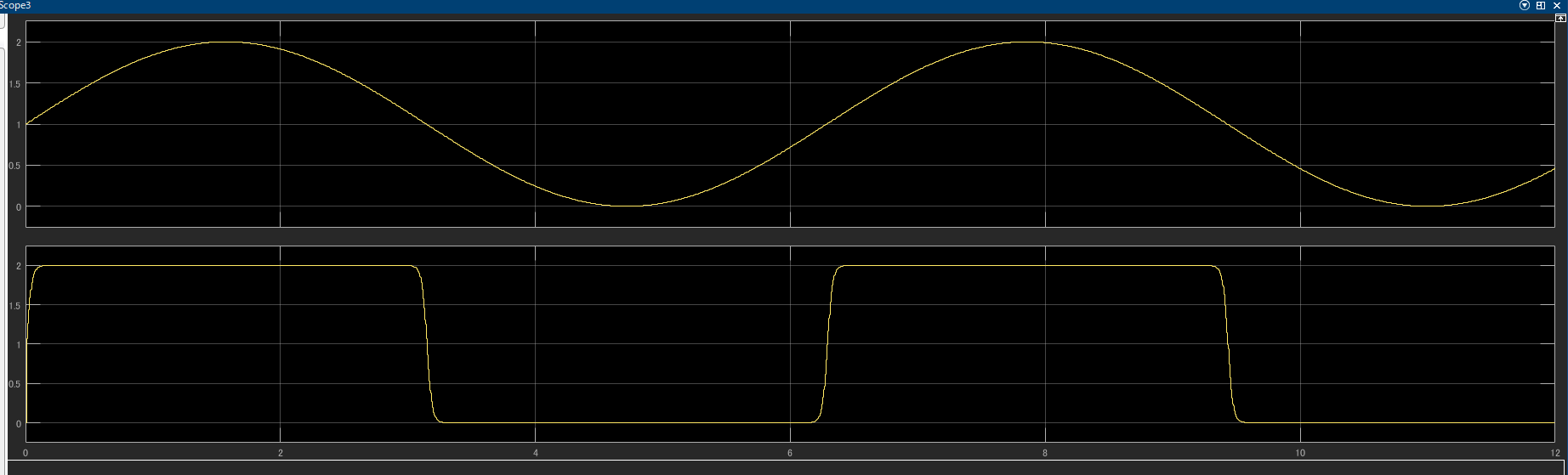
こちらの波形をMatlab SimulinkのMatlab関数を使ってシミュレーションできるようにする
シミュリンクでの基本的な構成
- NOT回路(Inverter)は、入力信号を反転させます。
- 遅れ要素(Delay)は、信号に一定の遅延を加える要素です。これにより、回路のタイミング特性をシミュレートできます。
- MATLAB Functionブロックを使用して、ロジスティック関数を実装し、出力電圧を計算します。
function Vout = CMOS_inverter(Vin)
    % 定数の設定 (Setting constants)
    Vdd = 2.0;  % 電源電圧 (Supply voltage)
    V_Tn = 1.0;  % NMOSのしきい値電圧 (Threshold voltage for NMOS)
    V_Tp = -1.0;  % PMOSのしきい値電圧 (Threshold voltage for PMOS)

    % 定数の設定 (Setting constants for mobility and oxide capacitance)
    mu_n = 600e-4;  % NMOSの移動度 (Electron mobility for NMOS)
    mu_p = 300e-4;  % PMOSの移動度 (Hole mobility for PMOS)
    C_ox = 3.45e-3;  % 酸化膜容量 (Oxide capacitance)

    % NMOSとPMOSのWとLを定義 (Define W and L for NMOS and PMOS)
    W_n = 10e-6;  % NMOSのチャンネル幅 (Channel width for NMOS)
    L_n = 2e-6;   % NMOSのチャンネル長 (Channel length for NMOS)
    W_p = 20e-6;  % PMOSのチャンネル幅 (Channel width for PMOS)
    L_p = 2e-6;   % PMOSのチャンネル長 (Channel length for PMOS)

    % βnとβpの計算 (Calculate βn and βp)
    beta_n = mu_n * C_ox * (W_n / L_n);
    beta_p = mu_p * C_ox * (W_p / L_p);

    % しきい値電圧Vthの計算 (Calculate Vth based on the provided formula)
    Vth = (Vdd + V_Tp + sqrt(beta_n / beta_p) * V_Tn) / (1 + sqrt(beta_n / beta_p));

    % ゲインの計算 (Calculate gain using the provided formula)
    gmp = 1e-3;  % PMOS transconductance (S)
    gmn = 1e-3;  % NMOS transconductance (S)
    rop = 10e3;  % PMOS output resistance (ohms)
    ron = 10e3;  % NMOS output resistance (ohms)
    gain = (gmp + gmn) / (1/rop + 1/ron);

    % ロジスティック関数を使ったCMOSインバーターの出力 (CMOS inverter output using logistic function)
    Vout = Vdd * (1 / (1 + exp(-gain * (Vth - Vin))));
end

import numpy as np
import matplotlib.pyplot as plt

# 定数の設定 (Setting constants for CMOS inverter)
Vdd = 1.0  # 電源電圧 (Supply voltage)
V_Tn = 1.0  # NMOSのしきい値電圧 (Threshold voltage for NMOS)
V_Tp = -1.0  # PMOSのしきい値電圧 (Threshold voltage for PMOS)

# 定数の設定 (Setting constants for mobility and oxide capacitance)
mu_n = 600e-4  # NMOSの移動度 (Electron mobility for NMOS)
mu_p = 300e-4  # PMOSの移動度 (Hole mobility for PMOS)
C_ox = 3.45e-3  # 酸化膜容量 (Oxide capacitance)

# NMOSとPMOSのWとLを定義 (Define W and L for NMOS and PMOS)
W_n = 10e-6  # NMOSのチャンネル幅 (Channel width for NMOS)
L_n = 2e-6   # NMOSのチャンネル長 (Channel length for NMOS)
W_p = 20e-6  # PMOSのチャンネル幅 (Channel width for PMOS)
L_p = 2e-6   # PMOSのチャンネル長 (Channel length for PMOS)

# βnとβpの計算 (Calculate βn and βp)
beta_n = mu_n * C_ox * (W_n / L_n)
beta_p = mu_p * C_ox * (W_p / L_p)

# しきい値電圧Vthの計算 (Calculate Vth based on the provided formula)
Vth = (Vdd + V_Tp + np.sqrt(beta_n / beta_p) * V_Tn) / (1 + np.sqrt(beta_n / beta_p))

# ゲインの計算 (Calculate gain using the provided formula)
gmp = 1e-3  # PMOS transconductance (S)
gmn = 1e-3  # NMOS transconductance (S)
rop = 10e3  # PMOS output resistance (ohms)
ron = 10e3  # NMOS output resistance (ohms)
gain = (gmp + gmn) / (1/rop + 1/ron)

# ロジスティック関数を使ったCMOSインバーターの出力 (CMOS inverter output using logistic function)
def logistic_inverter(Vin, Vdd, Vth, gain):
    return Vdd * (1 / (1 + np.exp(-gain * (Vth - Vin))))

# 入力電圧の範囲を設定 (Define input voltage range for CMOS inverter)
Vin = np.linspace(0, Vdd, 1000)

# 出力電圧の計算 (Calculate output voltage for CMOS inverter)
Vout = logistic_inverter(Vin, Vdd, Vth, gain)

# 定数の設定 (Setting constants for digital CMOS inverter)
A = 1    # パラメータA
B = 0.4  # パラメータB
C = 0.2  # パラメータC

# 点の設定 (Define the points for the digital CMOS inverter)
x_points = np.array([0, B, B+C, A])  # x座標
y_points = np.array([Vdd, Vdd, 0, 0])  # y座標

# プロット
plt.figure(figsize=(12, 6))

# CMOSインバーターのプロット (Plot the CMOS inverter transfer characteristics)
plt.subplot(1, 2, 1)
plt.plot(Vin, Vout, label='Vout vs. Vin (Logistic)', color='blue')
plt.title('CMOS Inverter Transfer Characteristics')
plt.xlabel('Input Voltage (Vin) [V]')
plt.ylabel('Output Voltage (Vout) [V]')
plt.grid(True)
plt.legend()

# デジタルCMOSインバーターのプロット (Plot the digital CMOS inverter characteristics)
plt.subplot(1, 2, 2)
plt.plot(x_points, y_points, marker='o', color='blue', label='Transfer Characteristics')
plt.title('Digital CMOS Inverter Characteristics')
plt.xlabel('Input Voltage (Vin) [V]')
plt.ylabel('Output Voltage (Vout) [V]')
plt.xlim(0, A)  # x軸の範囲設定 (Set x-axis range from 0 to A)
plt.grid(True)
plt.legend()

# レイアウト調整 (Adjust layout)
plt.tight_layout()
plt.show()