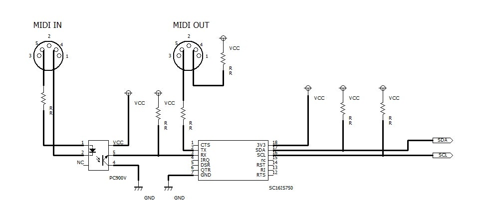
ArduinoのI2Cポートに、I2C to UART 変換を接続し、MIDIに入出力を行います。Arduino にはUARTポートが既にありますので、MIDIの入出力はできます。なのでもう1系統MIDIの入出力を付けるのは無駄な気はしますが、I2Cポートの実装練習のつもりでやってみました。2系統のMIDIを入出力するマージャーとして動作させることは可能です。
I2C to UART変換には、スイッチサイエンスさんで購入した、SC16IS750 シリアル-I2C ピッチ変換済みモジュール を使いました。
https://www.switch-science.com/catalog/2310/
SC16IS750/データシートは以下にあります。
https://goo.gl/JuiZih
フォトカップラーには秋月電商で購入したPC900Vを使いました。
http://akizukidenshi.com/catalog/g/gI-09813/
回路図
Include ヘッダー
Arduino でI2C を使う時には以下のヘッダーをInclude します。
# include <Wire.h>
I2C アドレスについて
**スイッチサイエンスさんのページにある通りですが、基板裏面にあるA1、A0のジャンパをカットし値を変えることによりI2C アドレスを変更できます。販売時はA1がVSS、A0がVDDに接続されているので、アドレスは0x98(1001 100X)**になります。
ところが、どうしてかわからないのですが、Arduino のプログラム上は、アドレスを一ビット右にシフトして使います。
const uint8_t slaveAddress = (0x98>>1);
レジスター
使うレジスターは以下の通りです。こちらもよくわからないのですが、取説に記載されているレジスターの番号を3ビット左へシフトアップして指定します。
// general register definition
const uint8_t RHR = (0x00<<3); //Receive Holding Register
const uint8_t THR = (0x00<<3); //Transmit Holding Register
const uint8_t FCR = (0x02<<3); //FIFO Control Register
const uint8_t LCR = (0x03<<3); //FLine Control Register
const uint8_t MCR = (0x04<<3); //Modem Control Register
const uint8_t LSR = (0x05<<3); //Line Status Register
const uint8_t RXLVL = (0x09<<3); //Receiver FIFO Level register

// special register set
const uint8_t DLL = (0x00<<3); //Division registers (DLL)
const uint8_t DLH = (0x01<<3); //Division registers (DLH)

//enhanced register set
const uint8_t EFR = (0x02<<3);
Receive Holding Register (RHR)
受信セクションは、受信保持レジスタ(RHR)と受信シフトレジスタ(RSR)から成っている。 RHRは実際には64バイトのFIFOです。 RSRは、シリアルデータをRX端子から受け取ります。データはパラレルデータに変換され、RHRに移動されます。受信セクションは、ライン制御レジスタによって制御されます。 FIFOがディスエイブルされている場合、FIFOのゼロ番地は、文字の格納に使用されます。
Transmit Holding Register (THR)
トランスミッタセクションは、送信保持レジスタ(THR)と送信シフトレジスタ(TSR)から成っている。 THRは実際には64バイトのFIFOです。 THRはデータを受け取り、それをTSRに移動すし、そこでシリアルデータに変換され、TXピンから出力される。 もしFIFOはディスエーブルされると、FIFOは依然としてバイトを保持しています。 オーバーフローが発生すると文字が失われます。
FIFO Control Register (FCR)
これは、書き込み専用のレジスタで、FIFOをイネーブルにしたり、FIFOをクリアしたり、
トランスミッタとレシーバのトリガレベルを受け取ります。表11にFIFO制御レジスタのビット設定を示します。
| Bit | Symbol | Description |
|---|---|---|
| 7:6 | FCR[7] (MSB) FCR[6] (LSB) |
RX trigger. RX FIFOのトリガーレベルを設定する 00 = 8 characters 01 = 16 characters 10 = 56 characters 11 = 60 characters |
| 5:4 | FCR[5] (MSB) FCR[4] (LSB) |
TX trigger. TX FIFOのトリガーレベルを設定する 00 = 8 spaces 01 = 16 spaces 10 = 32 spaces 11 = 56 spaces FCR [5:4]は、EFR [4]が設定されている場合にのみ、変更および有効にすることができます。これはTX FIFOのトリガーレベルは拡張された機能とみなされるからです。 |
| 3 | FCR[3] | reserved |
| 2 | FCR[2] | reset TX FIFO logic 0 = no FIFO transmit reset (normal default condition) logic 1の時、transmit FIFOをクリアし、FIFO level logicをリセットする。 (TSRはクリアもしくは変更されない). このビットはFIFOがクリアされた後、logic 0に戻る。 |
| 1 | FCR[1] | reset RX FIFO |
| 0 | FCR[0] | FIFO enable logic 0 = disable the transmit and receive FIFO (normal default condition) logic 1 = enable the transmit and receive FIFO |
FLine Control Register (LCR)
このレジスタは、データ通信形式を制御します。 word length、number of stop bits、およびparity typeは、適切なビットをLCRに書き込むことによって選択されます。 表12ライン制御レジスタのビット設定を示します。
| Bit | Symbol | Description |
|---|---|---|
| 7 | LCR[7] | divisor latch enable logic 0 = divisor latch disabled (normal default condition) logic 1 = divisor latch enabled |
| 6 | LCR[6] | イネーブルされると、ブレーク制御ビットによりブレーク条件が送信されます(TX出力は強制的にロジック0の状態になります)。この条件は、LCR [6]をロジック0に設定することによってディスエーブルされるまで存在します。. logic 0 = no TX break condition (normal default condition). logic 1 = transmitter output (TX)をlogic 0 に強制してcommunication terminal に回線断状態を警告する。 |
| 5 | LCR[5] | Set parity. LCR[5] selects the forced parity format (if LCR[3] = 1). logic 0 = parity is not forced (normal default condition). LCR[5] = logic 1 and LCR[4] = logic 0: parity bit is forced to a logical 1 for the transmit and receive data. LCR[5] = logic 1 and LCR[4] = logic 1: parity bit is forced to a logical 0 for the transmit and receive data. |
| 4 | LCR[4] | parity type select logic 0 = odd parity is generated (if LCR[3] = 1) logic 1 = even parity is generated (if LCR[3] = 1) |
| 3 | LCR[3] | parity enable logic 0 = no parity (normal default condition). logic 1 = a parity bit is generated during transmission and the receiver checks for received parity |
| 2 | LCR[2] | Number of stop bits. Specifies the number of stop bits. 0 to 1 stop bit (word length = 5, 6, 7, 8) 1 to 1.5 stop bits (word length = 5) 1 = 2 stop bits (word length = 6, 7, 8) |
| 1:0 | LCR[1] | Word length bits 1, 0. These two bits specify the word length to be transmitted or received; see Table 15. |
Modem Control Register (MCR)
MCRは、モード、データセット、またはモデムをエミュレートする周辺デバイスのインターフェイスを制御します。表17に、モデム制御レジスタのビット設定を示します。
| Bit | Symbol | Description |
|---|---|---|
| 7 | MSR[7] | clock divisor logic 0 = divide-by-1 clock input logic 1 = divide-by-4 clock input |
| 6 | MSR[6] | IrDA mode enable logic 0 = normal UART mode logic 1 = IrDA mode |
| 5 | MSR[5] | Xon Any logic 0 = disable Xon Any function logic 1 = enable Xon Any function |
| 4 | MSR[4] | enable loopback logic 0 = normal operating mode logic 1 = ローカルループバックモード(内部)を有効にします。 このモードでは、MCR [1:0]信号はMSR [4:5]にループバックされ、TX出力は内部的にRX入力にループバックされます。 |
| 3 | MSR[3] | reserved |
| 2 | MSR[2] | RTS logic 0 = force RTS output to inactive (HIGH) logic 1 = RTS出力をアクティブ(LOW)にします。 ループバックモードでは、MSR [4]を制御します。 自動RTSが有効な場合、RTS出力はハードウェアフロー制御によって制御されます。 |
| 1 | MSR[1] | ワード長ビット1,0。これら2つのビットは、送信または受信されるワード長を指定します。 表15を参照してください。 |
| 0 | MSR[0] | DTR[2]. IOControlレジスタのビット1を使用して、GPIO5がDTRモデム・ピンとして選択されている場合、DTRピンの状態は以下のように制御できます。 IOStateビット5への書き込みはこのピンに影響しません。 logic 0 = Force DTR output to inactive (HIGH) logic 1 = Force DTR output to active (LOW) |
Line Status Register (LSR)
The Line Status Register bit settings.
| Bit | Symbol | Description |
|---|---|---|
| 7 | LSR[7] | FIFO data error. logic 0 = no error (normal default condition) logic 1 = at least one parity error, framing error, or break indication is in the receiver FIFO. This bit is cleared when no more errors are present in the FIFO |
| 6 | LSR[6] | THR and TSR empty. This bit is the Transmit Empty indicator. logic 0 = transmitter hold and shift registers are not empty logic 1 = transmitter hold and shift registers are empty |
| 5 | LSR[5] | THR empty. This bit is the Transmit Holding Register Empty indicator. logic 0 = transmit hold register is not empty logic 1 = transmit hold register is empty. The host can now load up to 64 characters of data into the THR if the TX FIFO is enabled. |
| 4 | LSR[4] | break interrupt logic 0 = no break condition (normal default condition) logic 1 = a break condition occurred and associated character is 0x00, that is, RX was LOW for one character time frame |
| 3 | LSR[3] | framing error logic 0 = no framing error in data being read from RX FIFO (normal default condition). logic 1 = framing error occurred in data being read from RX FIFO, that is, received data did not have a valid stop bit |
| 2 | LSR[2] | parity error. logic 0 = no parity error (normal default condition) logic 1 = parity error in data being read from RX FIFO |
| 1 | LSR[1] | overrun error logic 0 = no overrun error (normal default condition) logic 1 = overrun error has occurred |
| 0 | LSR[0] | data in receiver logic 0 = no data in receive FIFO (normal default condition) logic 1 = at least one character in the RX FIFO |
Receiver FIFO Level register (RXLVL)
このレジスタは読み出し専用レジスタで、受信FIFOのフィルレベル つまり、RX FIFOの文字数を報告します。
| Bit | Symbol | Description |
|---|---|---|
| 7 | - | not used; set to zeros |
| 6:0 | RXLVL[6:0] | number of characters stored in RX FIFO, from 0 (0x00) to 64 (0x40) |
Division registers (DLL, DLH)
これらは、ボー・クロックの生成のための16ビット除数を格納する2つの8ビット・レジスタです。ボー・レート・ジェネレータでは、 DLHは除数の the most significant part を格納します。 DLLストア除数のthe least significant partを格納します。
ボーレイト
MIDI のボーレイトは31.25kbps ですので、
divisor = ((XTAL1 crystal input frequency)/prescaler)/desired baud rate 16
prescaler = 1, when MCR[7] is set to ‘0’ after reset (divide-by-1 clock selected)
prescaler = 4, when MCR[7] is set to ‘1’ after reset (divide-by-4 clock selected).
プログラム
MIDI IN とMIDI OUT を直結しています。MIDI INで受けたデータをそのまま出力します。プログラムを以下にまとめておきます。
# include <Wire.h>

const uint8_t slaveAddress = (0x98>>1);

// general register definition
const uint8_t THR = (0x00<<3);
const uint8_t RHR = (0x00<<3);
const uint8_t FCR = (0x02<<3);
const uint8_t LCR = (0x03<<3);
const uint8_t MCR = (0x04<<3);
const uint8_t LSR = (0x05<<3);
const uint8_t RXLVL = (0x09<<3);

// special register set
const uint8_t DLL = (0x00<<3);
const uint8_t DLH = (0x01<<3);

//enhanced register set
const uint8_t EFR = (0x02<<3);

uint8_t mData[8];

void setup() {
  // put your setup code here, to run once:
  uint8_t i2c_addr = slaveAddress;
  Wire.begin();

//Initialize Device
//divisor latch enabled
  Wire.beginTransmission(i2c_addr);
  Wire.write(LCR);
  Wire.write(0x83);
  Wire.endTransmission();
//set Baud Rate
  Wire.beginTransmission(i2c_addr);
  Wire.write(DLL);    //the least significant part
  Wire.write(24);
  Wire.endTransmission();
//set Baud Rate
  Wire.beginTransmission(i2c_addr);
  Wire.write(DLH);    //the most significant part
  Wire.write(0x0);
  Wire.endTransmission();
//divisor latch disabled
  Wire.beginTransmission(i2c_addr);
  Wire.write(LCR);
  Wire.write(0x03);
  Wire.endTransmission();
//reset TX and RX FIFO, enable the transmit and receive FIFO
  Wire.beginTransmission(i2c_addr);
  Wire.write(FCR);
  Wire.write(0x07);
  Wire.endTransmission();
}

int note=0;

void loop()
{
 uint8_t i2c_addr = slaveAddress;
 uint8_t i, n, data;

 Wire.beginTransmission(i2c_addr);
 Wire.write(LSR);
 Wire.endTransmission();
 Wire.requestFrom(i2c_addr, (uint8_t)1);
 data = Wire.read();

 if(data==0x61){ //at least one character in the RX FIFO
     Wire.beginTransmission(i2c_addr);
     Wire.write(RXLVL);
     Wire.endTransmission();
     Wire.requestFrom(i2c_addr, (uint8_t)1);
     n = Wire.read(); //読み込むデータの数

     Wire.beginTransmission(i2c_addr);
     Wire.write(RHR);
     Wire.endTransmission();
     Wire.requestFrom(i2c_addr, (uint8_t)n);
     for(i=0; i<n; i++){
          writeValue ( Wire.read() ); //読んだデータをそのままエコーバック
     }
 }
 delay(1);
}

void writeValue(uint8_t data){
     uint8_t i2c_addr = slaveAddress;
     Wire.beginTransmission(i2c_addr);
     Wire.write(THR);
     Wire.write(data);
     Wire.endTransmission();
}