動作環境
- Windows 10 Pro
- Vivado v2019.1
- CORA Z7 (Z7-07S)
概要
spi ADCにて8MS/sのデータをPLで取込み、そのデータをPSから任意タイミングで読みたい。
そのための予備的な技術情報整理を進めている。
今回はPLでBRAMに書き込み、PSから読み取る実装について整理しておく。
- Verilog HDLでBRAMに書き込む
- 接続相手はBlock Memory Generatorのブロック
- XSDKでPSからBRAMを読み取る
- メモリ指定読み出し
内容
Verilog HDLコード
bramWriter.v
`default_nettype none

/*
N個のデータをBRAMに書き込む

### 動作
リセット直後にN個のデータを書き込む
[SHIFT_VAL]からインクリメントされた値が書かれる
BRAM(Block Memory Generator IP)に接続して使用する
*/

module bramWriter
  (
    input wire clk,
    input wire resetn,
    output reg [31:0] addr_0,
    output reg [31:0] data_0,
    output reg [3:0] we_0 // Write Enable
  );

    localparam NUM_DATA = 128; // 書き込むデータ数
    localparam SHIFT_VAL = 100; // データをこの値からインクリメントする

    reg [31:0] counter; // 書き込みアドレス値に使う

    always @(posedge clk) begin
        if(resetn == 0) begin // リセット時の初期化
            counter <= 0;
            we_0 <= 4'h0;
        end else begin // 通常処理 (nominal path)
            if(counter < NUM_DATA) begin
                counter <= counter + 1;
                we_0 <= 4'hF; // Write Enable ON
            end else begin
                we_0 <= 4'h0; // Write Enable OFF
            end

            addr_0 <= {counter[29:0], 2'b00}; // 書き込みアドレス. 2'b00: アドレスを4ずつずらすため
            data_0 <= counter + SHIFT_VAL; // 書き込みデータ
        end
    end

endmodule // bramWriter

`default_nettype wire
テストベンチ
bramWriter_tb.v
`timescale 1ns / 1ps

module bramWriter_tb();

localparam STEP = 8;
localparam CLKNUM = 800;

// for input
reg CLK;
reg RSTN;
// for output
wire [31:0] addr0;
wire [31:0] data0;
wire [3:0] we0;

bramWriter bramWriter(
    .clk(CLK),
    .resetn(RSTN),
    .addr_0(addr0),
    .data_0(data0),
    .we_0(we0)
);

always begin
    CLK = 0; #(STEP/2);
    CLK = 1; #(STEP/2);
end

initial begin
    // 初期化
    RSTN = 1;
    #(STEP*5) RSTN = 0;
    #(STEP*5)  RSTN = 1;

    // CLK処理
    #(STEP*CLKNUM);
    $stop;
end

endmodule
Run Simulation結果
Run Simulationで100usまで実行した結果は以下の通り。
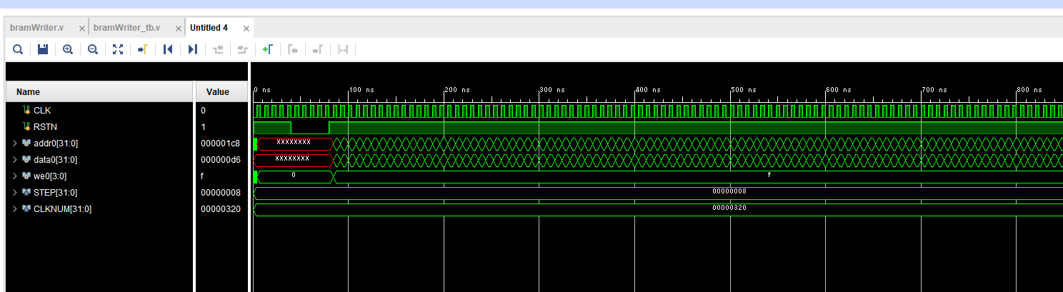
リセット解除直後の書き込みは以下の通り。

アドレス0x00に対して0x64(100)が書き込まれることを確認できた。
Block DesignとAddress
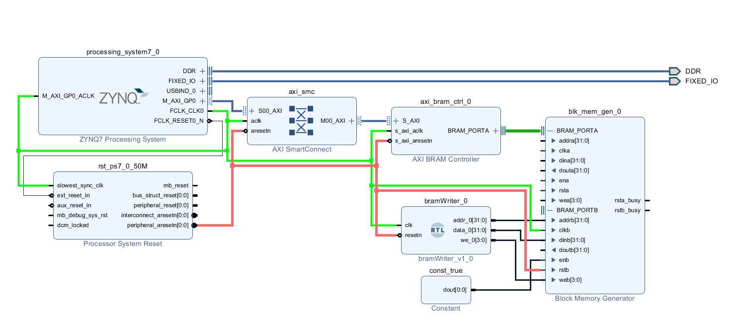
bramWriter.vを「Add Module to Block Design」してBlock Designに配置した。
Zynqを追加して、PSからBRAM読み取りできるように配置配線した。
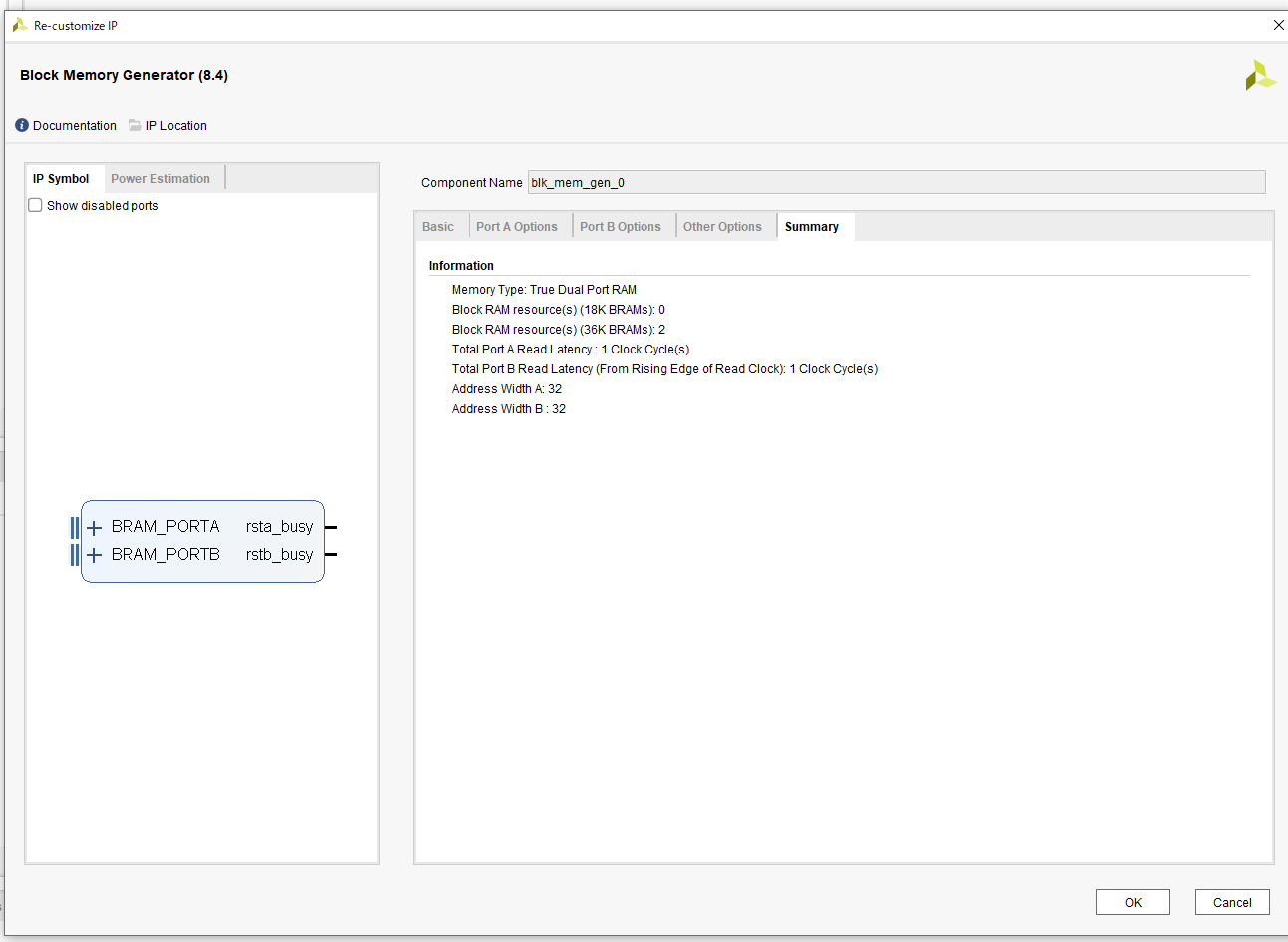
Block Memory Generatorの設定は以下の通り。
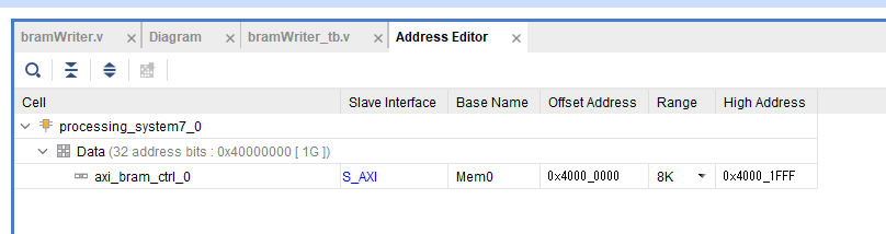
Address Editorペインは以下の通り。
XSDK実装
上記にてbitstreamを生成した。
以下のXSDK用コードを用意した。
xbram_example.c
# include <stdio.h>
# include "xil_printf.h"
# include "xparameters.h"
# include "xbram.h"

# define BRAM_BASE  (XPAR_BRAM_0_BASEADDR)

int main()
{
    printf("Hello 1030\r\n");

    u32 *brams = (u32 *)BRAM_BASE; // 配列アクセス用
    for(int idx = 0; idx < 100; idx++) {
        printf("value in BRAM %ld\r\n", brams[idx]);
    }

    return 0;
}
実行結果

値が100からインクリメントされることを確認できた(正常)。
関連
- PG058 : Block Memory Generator v8.4